Solid Solution Diagram Gan And Gaas Generative Adversarial N
Gan phase Energy level diagram of gan and gaas based hemt. Solid liquid gas cut out stock images & pictures
Solid-solution phase diagram of Ga 1−x In x As. | Download Scientific
Gaas wafers Study the diagram shown on the next page (figure -1). Schematic diagram of a method for controlling the polarity of gan using
Solid solution phase diagram
Matter states chemistry solid state gas liquid solids three liquids gases different year revision gcse each general learnGan equilibrium pressures line temperature Gaas phase diagram freiberger wafer(color online) schematic diagram of the (a) gaas single-junction and.
9.2.1 bulk crystalsEstimates of the ga diffusion length, s ,ga , on gan. the solid line Binary solid solutionsGenerative adversarial networks(gans): complete guide to gans.

Physical review letters on twitter: "the structure of the solid-liquid
Phase solid solutions diagramsPhase diagrams 2 Solid liquid gas drawingEnergy level diagram of gan and gaas based hemt..
Plasma moleculesDay 27:使用keras撰寫 生成式對抗網路(gan) Solid solution phase diagramExtracted (symbols) and calculated (solid lines) results of gan.

Solid-solution phase diagram of ga 1−x in x as.
Gaas mixture crystalsSchematic diagram of the solid solution model. a sample is divided into Solved problem-5 solid state physics (structure of gan) aChemistry year 7.
Liquid to gas is calledFigure s1. p-type gaas and gan used to reveal the distinctive current Gaas crystalsPhase solid synthesis state diagram diagrams component solutions example materials ppt.

Phase diagrams for the gan ͑ 0001 ͒ surface as a function of al and ga
Igneous petrology series: lesson 5Gan diffusion growth temperature estimates structural Fig. s1: schematic diagram of a solid solution. the figure to the leftGan phase diagram at pressures between 1 and 100 bar. equilibrium line.
(a) schematic diagram of gan/gaas interface energy band; (b) ldos ofGan solutions: devices to solid state hpas Solids liquids gases chartTriangle diagram state of matter liquid gas, diagram, angle, text.

(a) Schematic diagram of GaN/GaAs interface energy band; (b) LDOS of

9.2.1 Bulk Crystals

Estimates of the Ga diffusion length, S ,Ga , on GaN. The solid line

Solid liquid gas Cut Out Stock Images & Pictures - Alamy

Energy level diagram of GaN and GaAs based HEMT. | Download Scientific

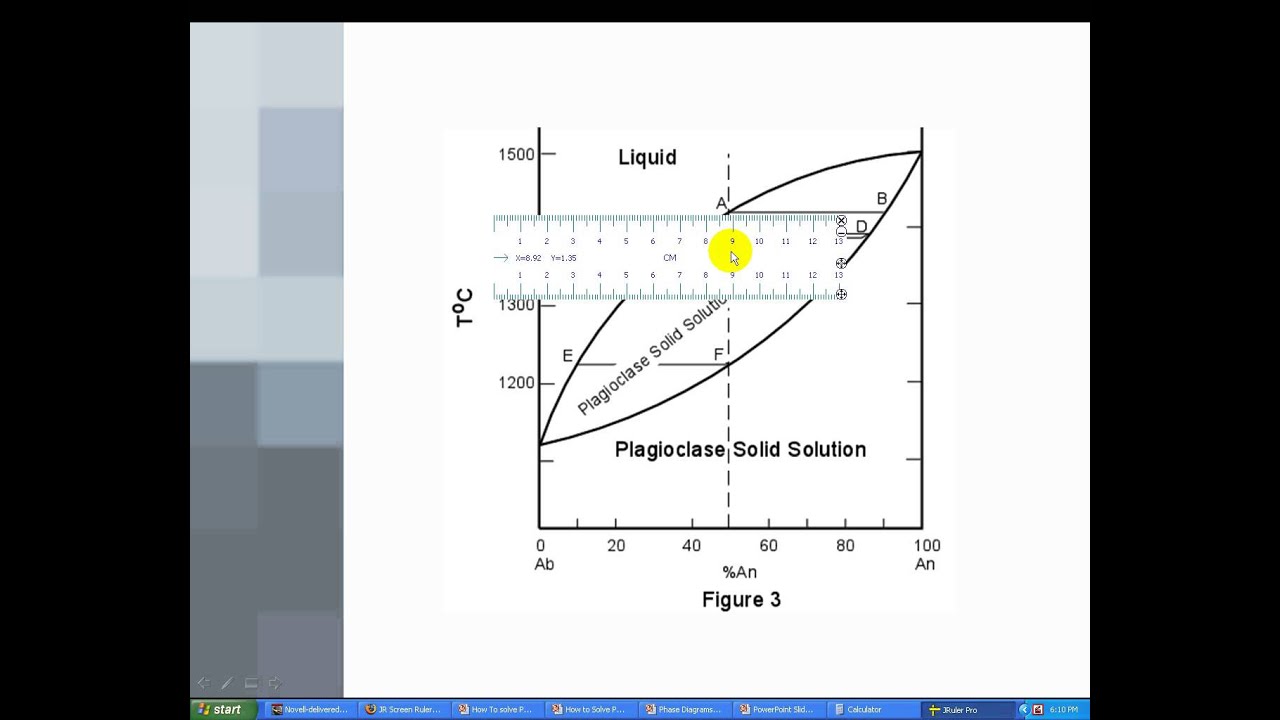
Solid Solution Phase Diagram | Diagram, Solutions, Pie chart

Figure S1. P-type GaAs and GaN used to reveal the distinctive current

Schematic diagram of a method for controlling the polarity of GaN using